| README.md | ||
SOC Design For Testing Digital IP chips (RISC V and SRAM)
This Project explains the importance of components used in the PCB design and also how data flows within the design.
Table of Contents
- Brief Introduction to Testing flow
- Introduction to FT2232H
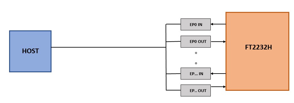
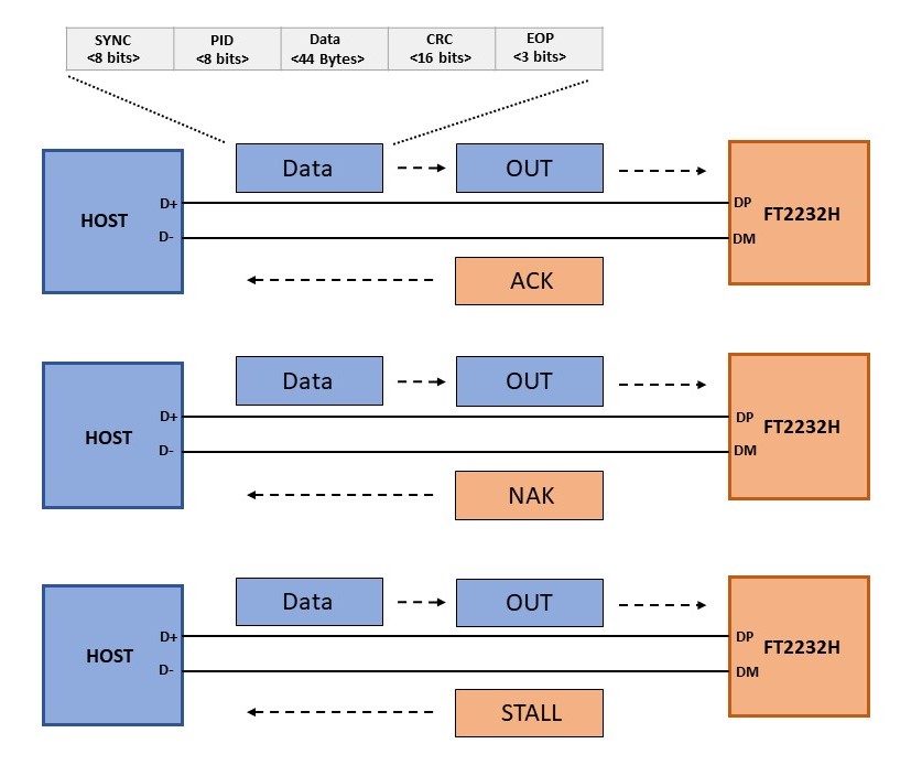
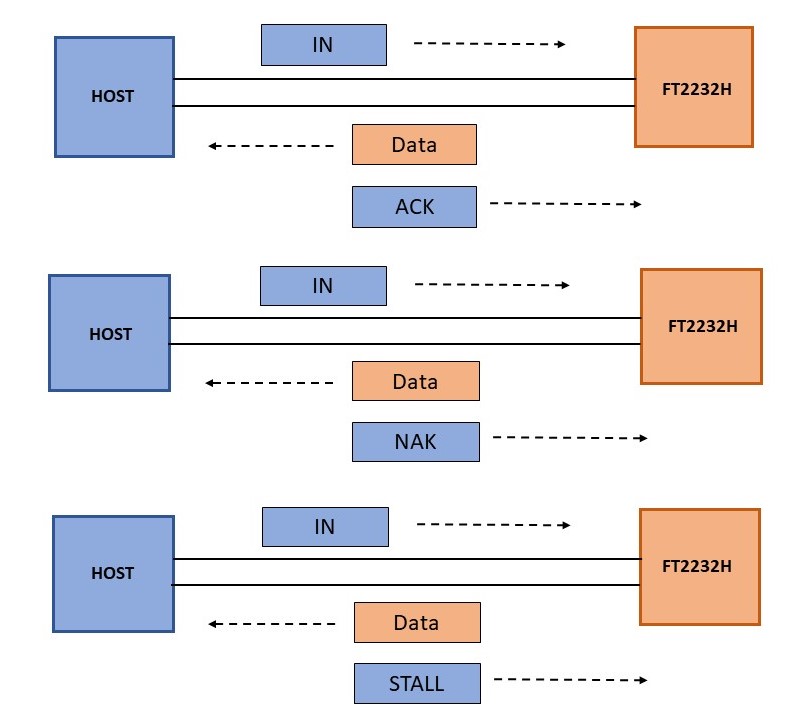
- Data flow from USB port to FT2232H
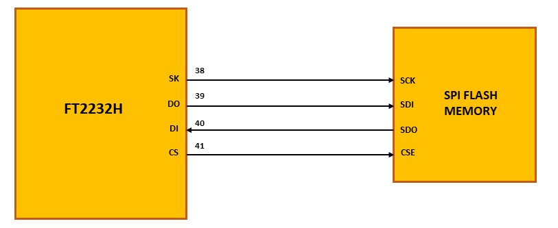
- Data flow from FT2232H to SPI flash memory
- Future work
- Acknowledgements
Brief Introduction to Testing flow
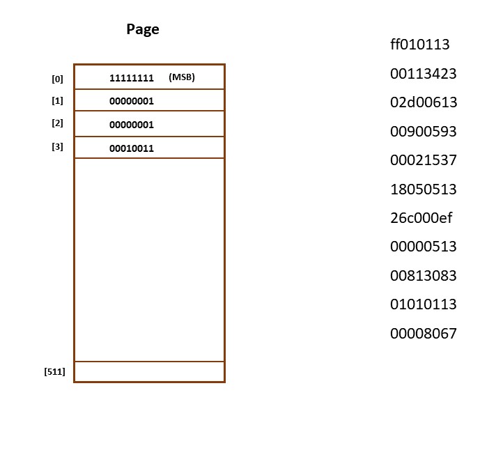
An IDE ( Integrated Development Environment) is used for programming the PCB design. For an IDE to recognize the hardware board, a Board Support Package(BSP) which includes hardware description and linker files for memory mapping are used and after programming, the hex files are generated. The resultant bitstream is passed to the following PCB design.
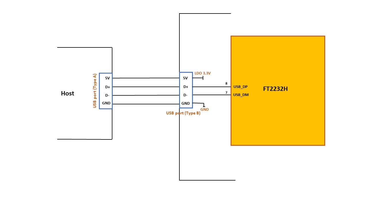
Introduction to FT2232H
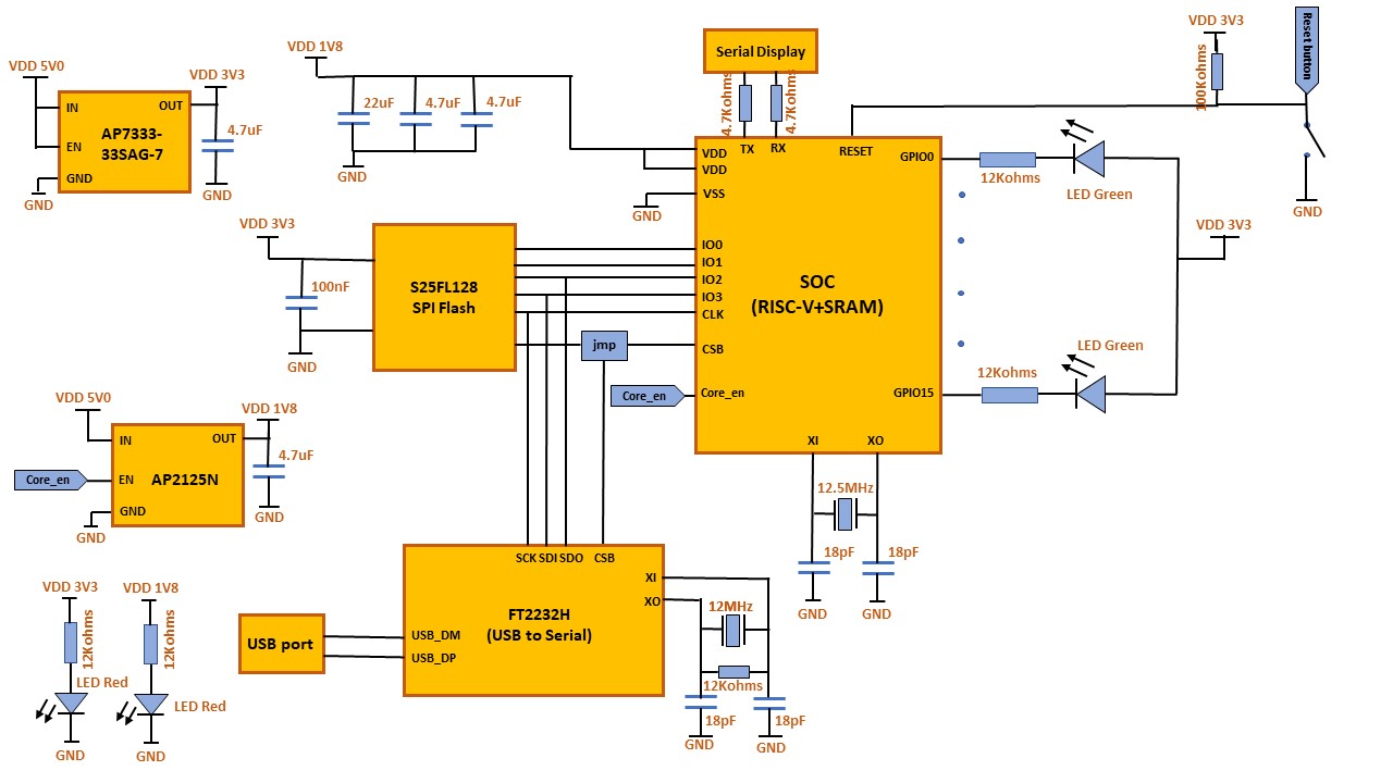
The serial port of the computer usually meets RS-232 standard. It has signal voltage swing of around -13 to +13V. The PCB design uses TTL serial (Transistor-Transistor logic) which has signal voltage level between 0 and VDD ( 3.3V/1.8V). A common communication protocol is needed for data transfer, hence FT2232H is used for converting USB to serial converter.