| Images | ||
| README.md | ||
SOC Design For Testing Digital IP chips (RISC V and SRAM)
This project explains the importance of components used in the PCB design based on the RISC V and SRAM are on the single chip for testing the entire PCB board and also explains how data flows within the design right from writing the code in C in a Software IDE/SDK to transmitting the code to the Flash Memory.
Table of Contents
- Brief Introduction to Testing flow
- Introduction to FT2232H
- Data transfer from USB port to FT2232H
- Data transfer from FT2232H to SPI flash memory
- Future work
- Acknowledgements
Brief Introduction to Testing flow
An IDE ( Integrated Development Environment) is used for programming the PCB design. For an IDE to recognize the hardware board, a Board Support Package(BSP) which includes hardware description and linker files for memory mapping are used and after programming, the hex files are generated. The resultant bitstream is passed to the following PCB design.
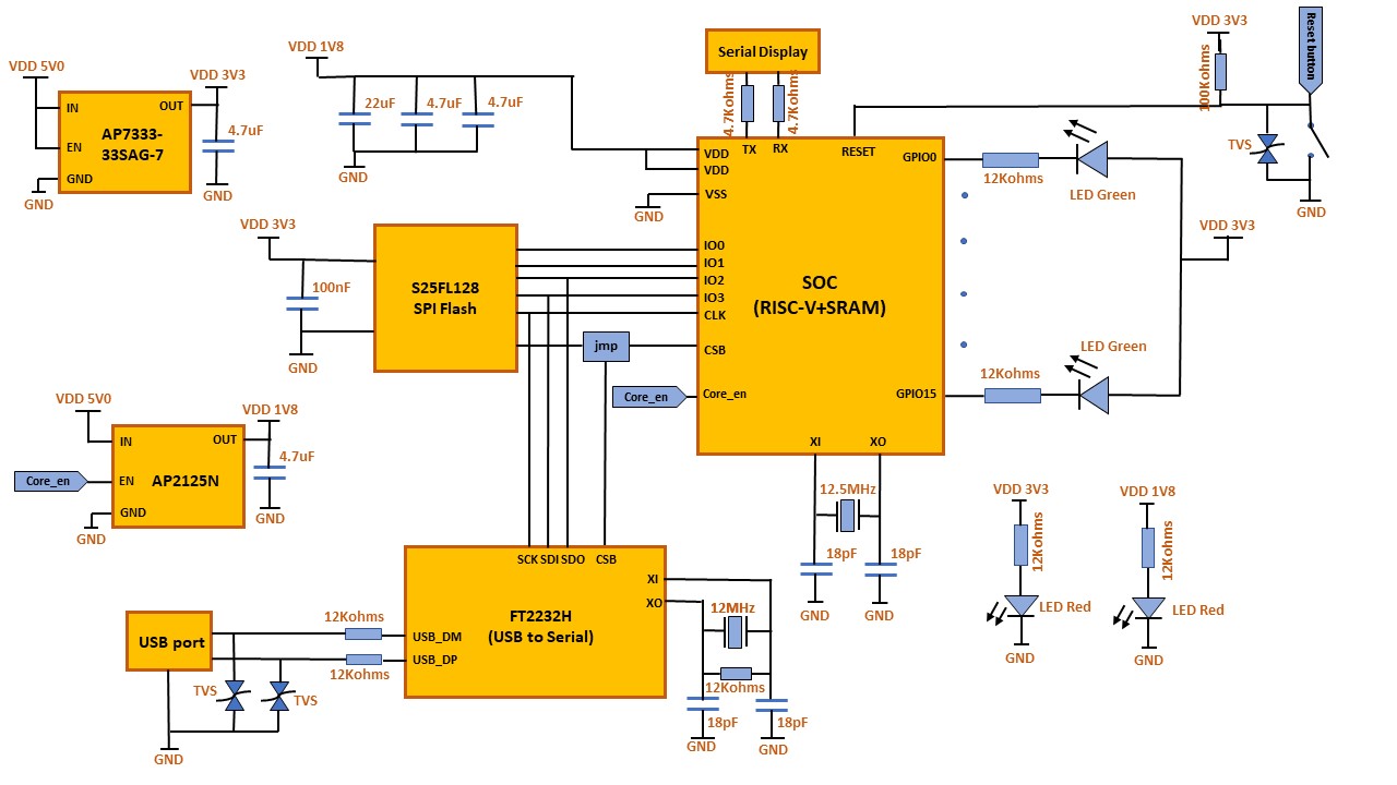
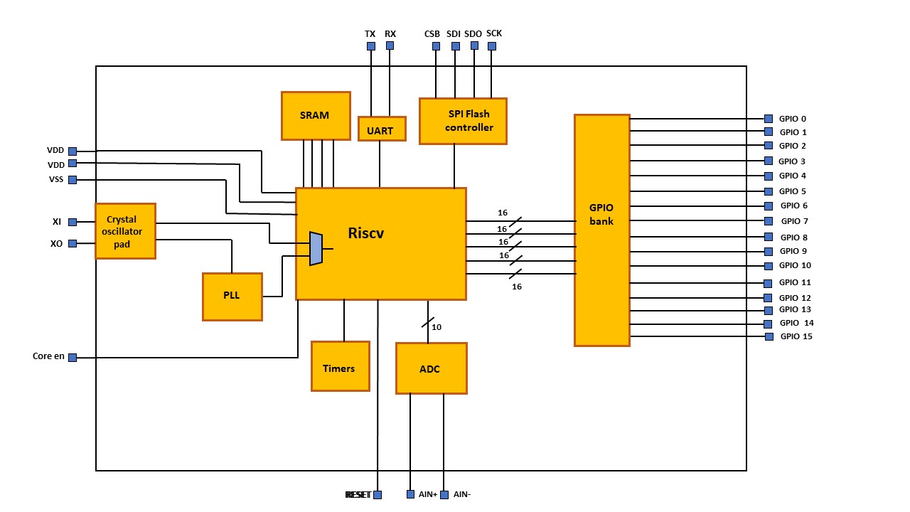
The internal SOC consists of RISC V, SRAM, GPIOs and PLL which can be provided by sky130 PDK and rest of the components like ADC, UART module and timers has to be included in the Bill Of Materials (BOM).
Introduction to FT2232H
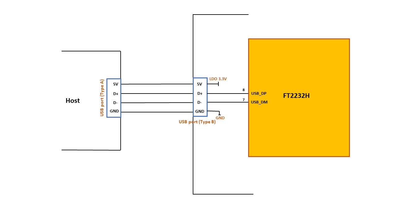
The serial port of the computer usually meets RS-232 standard. It has signal voltage swing of around -13 to +13V. The PCB design uses TTL serial (Transistor-Transistor logic) which has signal voltage level between 0 and VDD ( 3.3V/1.8V). A common communication protocol is needed for data transfer i.e data has to be transferred at same baud rate and at same endianness. hence FT2232H is used for converting USB to serial converter.
For the data transfer from host to the target (board), we connect USB cable ( USB type A to the PC and Type B to the board). USB has 4 signals, 5V power supply signal, ground and 2 data signals(D+ and D-).
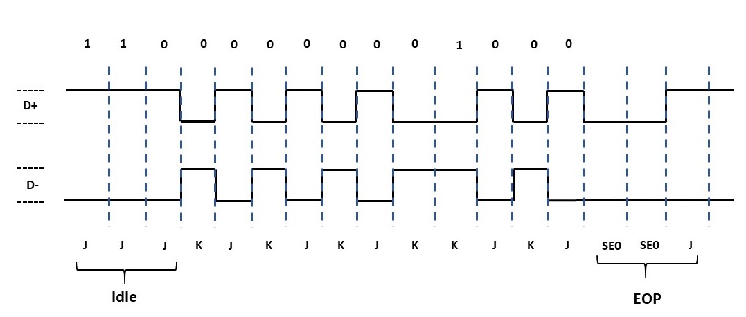
The data is transferred from these two data lines using NRZI encoding.
Data transfer from USB port to FT2232H
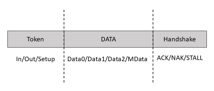
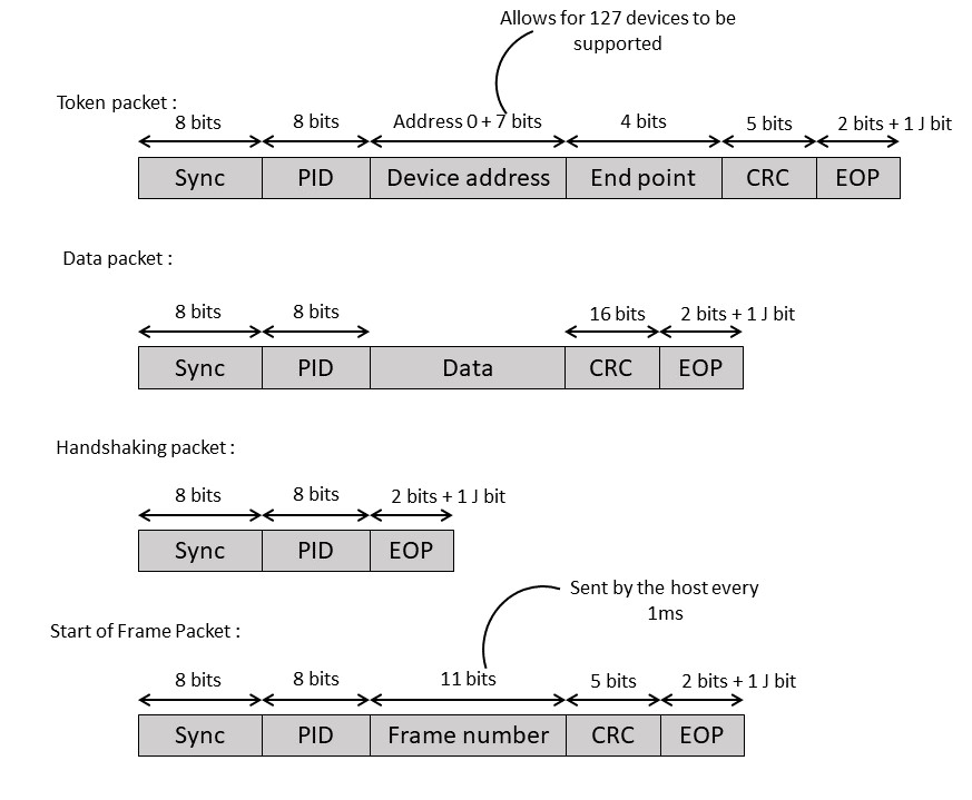
According to USB communication protocol, data is sent through packets. It consists of 3 common packets.
Data field can carry varying size of data depending upon the speed at which data is transferred.
- For low speed devices, data can be upto 8B
- For full speed devices, data can be upto 1023B
- For high speed devices, data can be upto 1024B
Basically, the data transaction can be done in 4 types:
- Control: It is generally used by host for sending commands and parameters.
- Interrupt: It is used by devices for sending small amounts of data. It is a polled message from the host to request specific data of the device
- Bulk: this is used by devices for sending large amounts of data.
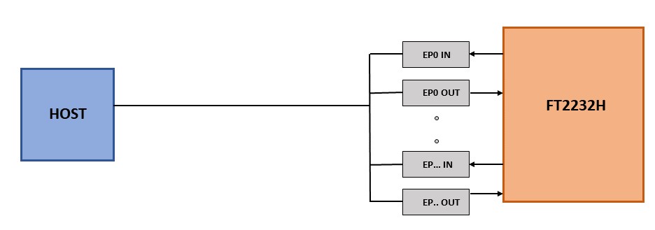
- Isochronous: this is generally used by devices like audio channels etc, for streaming real time data. FTDI supports bulk data transaction. Data is sent through endpoint buffers within the device. FT2232H can have a maximum packet size of 512B.
The following example code is considered to demonstrate how the data flows from one block to other. ( Image courtesy: Shivanishah/riscv)
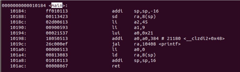
The example code has a bitstream of 44bytes. This is sent from host to device through data packet in data field.
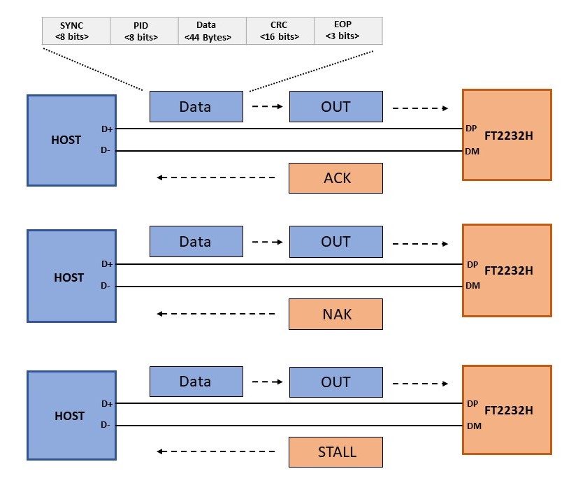
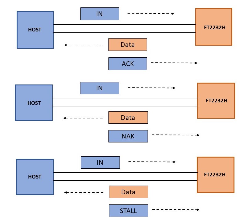
The data transfer from device to the host is done when host is ready to accept data, it sends token packet. The device then sends data.
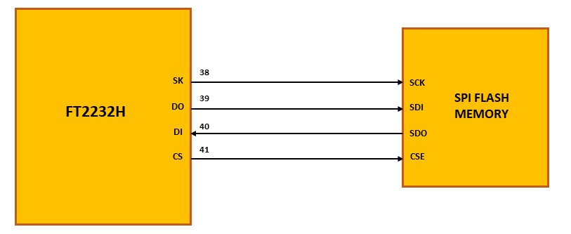
Data transfer from FT2232H to SPI flash memory
FT2232H has multiple configurations like synchronous bitbang interface, asynchronous bitbang interface and MPSSE (Multi-Protocol Synchronous Serial Engine) interface. MPSSE mode allows communication with different types of synchronous devices like SPI, I2C, JTAG etc.
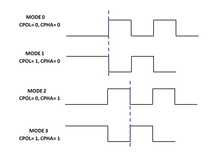
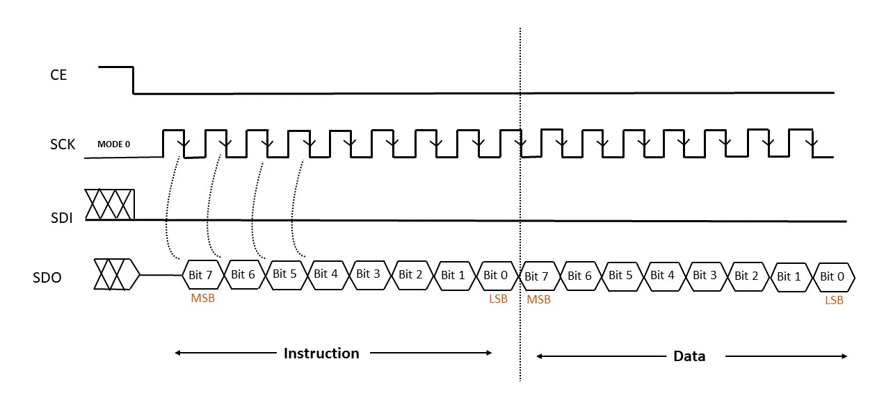
SPI communication has 4 modes for data transfer depending on clock polarity (CPOL) and clock phase (CPHA). FTDI device can only support mode 0 and mode 2 whereas flash memory (S25FL128S) has only 2 clocking modes i.e mode 0 and mode 3.
The data transfer between FT2232H and S25FL128S is done in the form of units called commands. These commands consist of instructions which tells the device operation and may also have address, latency period followed by data. The input data into the device is always latched in at the rising edge of the SCK signal and the output data is always available from the falling edge of the SCK clock signal.
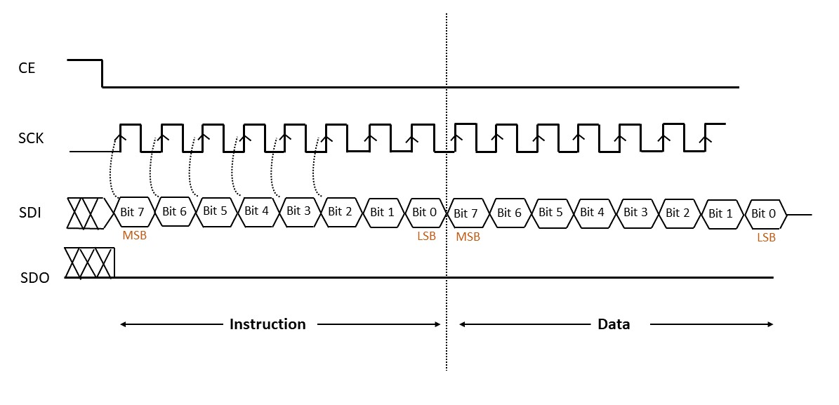
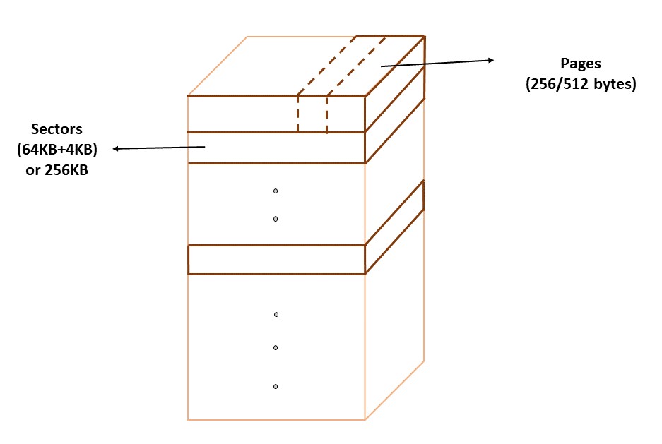
The memory is divided into sectors either a combination of 64KB and 4KB or a size of 256KB. For a sector size of 256KB, there can be total of 64 sectors for the memory and each sector is again divided into pages. Each page size can be a maximum of 512B.
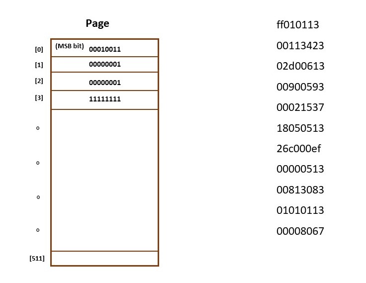
The data is transferred in byte units and after each byte transmission the address byte is incremented automatically. Also, data is tranfer in little endian fashion.For writing the data, the maximum data that can be written in one operation is upto 512B. For more data transfer, again instruction followed by address is sent.
Future work
- Data transfer from flash memory to SOC and rest of the blocks.
Acknowledgements
Kunal Ghosh, Co-founder (VSD Corp. Pvt. Ltd)